
Diamond Foundry Unveils World-First 200mm Single-Crystal Diamond Wafer to Combat Severe AI Chip Thermal Limits

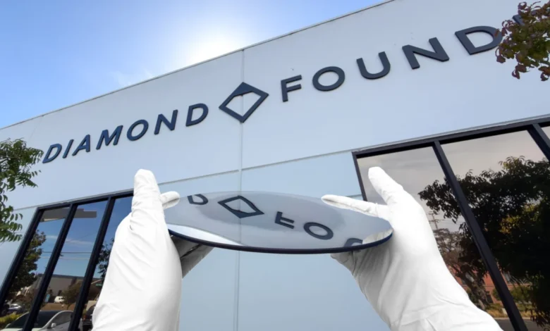
The relentless scaling of modern semiconductor architectures, driven primarily by the astronomical computational demands of artificial intelligence workloads, has precipitated a severe thermodynamic crisis within the hardware industry. As processors push higher power densities and thermal design power (TDP) thresholds exceed traditional cooling capacities, the search for revolutionary thermal management materials has intensified. Addressing this unprecedented industry bottleneck, lab-grown diamond producer Diamond Foundry has announced the successful manufacture of the world’s first 200mm single-crystal diamond (SCD) wafer. This technological milestone marks the formal entry of diamond into the mainstream, wafer-scale semiconductor fabrication era, offering a material that possesses thermal conductivity at least five times greater than that of copper—long considered the gold standard for passive and active heat dissipation in electronics.
Main Facts and Technological Breakthrough
The newly unveiled 200mm single-crystal diamond wafer represents a monumental shift in materials science and semiconductor manufacturing. Historically, diamonds have been recognized as having exceptional thermal capabilities, largely due to the unique rigidity of the carbon-carbon covalent bond lattice, which facilitates exceptionally efficient phonon transport. While copper exhibits a thermal conductivity of approximately 400 watts per meter-kelvin (W/m·K) at room temperature, high-purity single-crystal diamond can achieve thermal conductivities exceeding 2,000 W/m·K.
Despite these stellar physical properties, commercializing diamond for semiconductor applications has historically been hindered by prohibitive manufacturing constraints. Diamonds are notoriously difficult to synthesize in large, uniform structures, let alone at dimensions compatible with standard industrial semiconductor fabrication lines. Wafer sizes in the semiconductor industry dictate manufacturing efficiency and compatibility with photolithography tools, etching chambers, and packaging equipment. By achieving a diameter of 200 millimetres (approximately 8 inches), Diamond Foundry has aligned its diamond production with mature semiconductor fabrication standards, specifically the wafer sizes commonly utilized by legacy and specialty semiconductor fabs worldwide.
The company officially highlighted the breakthrough on its corporate insights portal, declaring that single-crystal diamond has finally crossed the threshold into the wafer-scale era. This transition bridges the gap between boutique, laboratory-scale diamond synthesis and mass-production-ready semiconductor components.
Chronology of Diamond Synthesis in Electronics
The journey toward integrating diamond into mainstream electronics spans several decades, characterized by incremental advancements in chemical vapor deposition (CVD) and high-pressure high-temperature (HPHT) synthesis techniques.
During the late 20th century, synthetic diamonds were primarily utilized for industrial cutting tools, abrasive coatings, and optical windows due to their extreme hardness and optical transparency. However, materials scientists quickly recognized the potential of diamond as an ultimate semiconductor substrate and heat spreader. The primary obstacle was the inability to grow large-area single crystals; diamonds grown via HPHT were typically restricted to small, millimeter-scale cubes, while early CVD techniques produced polycrystalline diamond films. Polycrystalline diamond, while thermally conductive, suffers from phonon scattering at grain boundaries, which significantly degrades its thermal and electrical performance compared to single-crystal variants.
In the 2010s, advancements in plasma-assisted chemical vapor deposition allowed researchers to grow thicker, higher-purity single-crystal diamond plates by heteroepitaxially or homoepitaxially depositing carbon atoms onto suitable seed substrates. Despite these improvements, scaling these crystals beyond a few square centimeters remained economically and technically unfeasible for high-volume semiconductor integration.
Over the past five years, companies like Diamond Foundry scaled up proprietary plasma reactor technology, enabling rapid vertical and lateral growth of diamond lattices. The culmination of this multi-year research and development cycle is the 200mm single-crystal wafer announced today, which bypasses the restrictive size barriers that previously relegated diamond to niche thermal management applications, such as high-frequency radio frequency (RF) power amplifiers and specialized laser diodes.
Supporting Data and Thermodynamic Comparison
To understand the profound implications of Diamond Foundry’s 200mm SCD wafer, one must examine the governing metrics of thermal management in modern microelectronics. Modern graphics processing units (GPUs) and artificial intelligence accelerators, such as enterprise-grade machine learning training clusters, regularly dissipate hundreds—and in some cases over a thousand—watts of thermal energy within a footprint smaller than a standard postcard.
Traditional thermal solutions rely on a cascading hierarchy of cooling materials: silicon dies are mounted to integrated heat spreaders (IHS) typically made of nickel-plated copper, which in turn transfer heat via thermal interface materials (TIMs) to aluminum or copper fin stacks attached to liquid cooling loops or massive air coolers. However, copper and aluminum face critical limitations when subjected to extreme heat fluxes. Copper’s thermal conductivity of ~400 W/m·K, while adequate for traditional central processing units (CPUs), struggles to prevent localized hot spots on modern AI processors where heat generation exceeds 100 watts per square centimeter.
Diamond outperforms all conventional metals and alloys used in semiconductor packaging:
- Aluminum: ~205 W/m·K
- Copper: ~401 W/m·K
- Silver: ~429 W/m·K
- Polycrystalline Diamond: ~1,000 to 1,800 W/m·K (depending on grain structure and purity)
- Single-Crystal Diamond: 2,000 to 2,200+ W/m·K
Furthermore, diamond possesses an extremely low thermal expansion coefficient and high electrical insulation properties when un-doped, making it an ideal substrate for direct-die cooling. By placing a diamond heat spreader or substrate directly in contact with, or integrated into, the semiconductor die, heat can be removed laterally and vertically away from critical transistor junctions at speeds previously unattainable with metallic solutions.
Industry Reactions and Strategic Implications
While direct quotes from competing semiconductor fabrication foundries and major fabless designers like Nvidia, AMD, and Intel remain measured given the early commercial availability of the 200mm wafers, industry analysts have universally recognized the announcement as a strategic turning point.
Thermal engineers across the high-performance computing (HPC) sector have long advocated for diamond-based cooling architectures, but supply chain limitations and cost per square millimeter have kept the technology out of consumer and mainstream enterprise hardware. By demonstrating 200mm wafer capability, Diamond Foundry has signaled to the market that economies of scale are now achievable.
From a manufacturing perspective, a 200mm wafer format allows integrated device manufacturers (IDMs) and outsourced semiconductor assembly and test (OSAT) facilities to utilize existing toolsets designed for 8-inch silicon wafers. This compatibility drastically reduces the capital expenditure required for packaging houses to adopt diamond-based thermal solutions. Rather than engineering entirely bespoke robotics and handling mechanisms for irregularly shaped diamond shards, fabs can leverage mature lithography, dicing, and handling infrastructure.
Broader Impact on AI Hardware and Power Electronics
The timing of Diamond Foundry’s announcement is directly linked to the exponential growth of artificial intelligence. Data centers housing clusters of AI accelerators face severe power provisioning and cooling constraints. Liquid cooling has become mandatory for leading-edge AI hardware, yet even advanced liquid-to-chip cooling blocks encounter thermal resistance barriers at the interface between the silicon die and the cooling medium.
Integrating single-crystal diamond layers directly into semiconductor packaging or utilizing diamond substrates for wide-bandgap semiconductors—such as gallium nitride (GaN) and silicon carbide (SiC) used in power electronics—promises to alleviate these thermal bottlenecks. Wide-bandgap semiconductors operate at higher voltages, frequencies, and temperatures than traditional silicon, but their deployment is frequently throttled by thermal management issues. Diamond substrates provide the ultimate thermal sink, enabling power electronics to operate at maximum efficiency without thermal degradation or catastrophic failure.
Furthermore, the implications extend into consumer computing, high-frequency telecommunications, and electric vehicle (EV) powertrains. As power densities continue to escalate across all computing domains, the thermal limits of silicon and copper are fast approaching asymptotic boundaries.
Conclusion and Outlook
Diamond Foundry’s introduction of the world’s first 200mm single-crystal diamond wafer transforms diamond from a geological rarity and niche industrial abrasive into a foundational material for the next generation of semiconductor engineering. By scaling diamond production to dimensions compatible with industrial fabrication lines, the company has cleared the primary hurdle preventing the widespread adoption of diamond-based thermal management. As the semiconductor industry grapples with the punishing thermal realities of the artificial intelligence era, wafer-scale single-crystal diamond stands out as a critical technological pillar capable of sustaining future computational growth.