
GlobalFoundries VP details FDX Fusion technology, sporting 7nm-class performance without the need for EUV tools —…

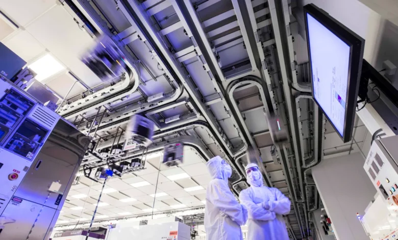
GlobalFoundries has unveiled strategic details regarding its next-generation semiconductor manufacturing framework, known as FDX Fusion. According to senior leadership at the company, this ambitious initiative aims to deliver performance metrics traditionally associated with the 7-nanometer (nm) class of processors, but with a major caveat and distinct manufacturing advantage: it achieves this level of performance without requiring extreme ultraviolet (EUV) lithography tools, relying instead on planar transistor architectures. While the resulting product operates at a comparatively lower transistor density than standard 7nm FinFET or gate-all-around (GAA) nodes, the omission of EUV equipment could drastically alter the cost structure and production accessibility for high-performance specialty chips. GlobalFoundries has targeted 2030 as the milestone for initiating high-volume manufacturing (HVM) for the FDX Fusion platform.
The semiconductor industry has spent the last decade racing toward increasingly complex manufacturing nodes, driven by the relentless pursuit of Moore’s Law. This trajectory has made extreme ultraviolet lithography an absolute prerequisite for advanced logic chips, with companies like TSMC, Samsung, and Intel investing tens of billions of dollars into high-NA and standard EUV scanners. However, the soaring cost of these tools has created a massive financial barrier for chip designers, limiting sub-7nm development to a handful of deeply capitalized entities. GlobalFoundries’ FDX Fusion approach represents a calculated divergence from this mainstream roadmap, targeting an intersection of performance, power efficiency, and cost-effectiveness that appeals to automotive, industrial, and specialized computing sectors that do not necessarily require ultra-dense packaging.
Understanding the Architecture: Planar Transistors Meet Advanced Performance
To comprehend the significance of FDX Fusion, one must examine the fundamental shift in transistor design over the past fifteen years. As nodes shrank below 20nm, traditional planar (flat) transistors suffered from severe leakage currents and short-channel effects, forcing the industry to transition to 3D architectures like FinFETs and, more recently, nanosheet or gate-all-around (GAA) transistors. These 3D structures drastically improved electrical control and power efficiency at microscopic scales, but they also introduced immense manufacturing complexity.
GlobalFoundries’ FDX (Fully Depleted Silicon-on-Insulator) technology has long stood as an alternative path. By utilizing a thin layer of insulator beneath the channel, FD-SOI provides exceptional energy efficiency, radiation tolerance, and thermal stability without the extreme complexity of 3D FinFET fabrication. With FDX Fusion, the company is pushing this foundational concept significantly further. By combining advanced materials science, optimized strained silicon techniques, and innovative circuit design methodologies, GlobalFoundries aims to extract 7nm-class performance metrics—such as operating frequencies and power envelopes—out of a modernized planar or modified FD-SOI structure.
Industry analysts point out that while a lower transistor density means that chips built on FDX Fusion will have larger die sizes compared to a true 7nm FinFET node from a foundry like TSMC, the absence of EUV steps dramatically reduces mask costs, cycle times, and equipment depreciation expenses. For many applications, a larger die that is significantly cheaper to produce and immune to the supply bottlenecks associated with ASML’s EUV machines presents a highly attractive economic proposition.
The Strategic Decision to Bypass EUV Lithography
The most disruptive element of the FDX Fusion disclosure is the deliberate avoidance of EUV tools. Extreme ultraviolet lithography systems are arguably the most complex machines ever built by humanity, requiring multi-million-dollar mirrors, high-powered plasma light sources, and ultra-clean environments. Their scarcity and astronomical price tags have driven up wafer costs across the board.
By refining deep ultraviolet (DUV) immersion lithography—potentially through multi-patterning techniques such as Self-Aligned Quadruple Patterning (SAQP)—GlobalFoundries aims to bypass the EUV bottleneck entirely. This strategy mirrors historical shifts where foundries stretched older lithography generations to their absolute physical limits before committing to expensive optical transitions.
From a geopolitical and supply chain perspective, avoiding EUV could also insulate GlobalFoundries’ customers from certain export controls, intellectual property bottlenecks, and manufacturing dependencies that heavily govern advanced node production today. Although DUV multi-patterning introduces its own manufacturing challenges—such as tighter overlay tolerances, defect management, and increased mask counts—GlobalFoundries believes that the net economic benefit will outweigh these technical hurdles by the time production scales up.
Chronology and the Road to 2030
The announcement of FDX Fusion is the latest step in a multi-year evolutionary roadmap for GlobalFoundries’ proprietary FD-SOI technology platform.
- Early 2010s: The foundational FD-SOI technology was originally pioneered by STMicroelectronics and later heavily invested in by GlobalFoundries, with production facilities established primarily in Dresden, Germany.
- Mid-to-Late 2010s: GlobalFoundries successfully commercialized its 22FDX and 12FDX nodes, securing design wins in IoT, automotive radar, and low-power microcontrollers due to the technology’s inherent energy efficiency and body-biasing capabilities.
- 2021–2023: Following its initial public offering (IPO), GlobalFoundries shifted its strategic focus away from the ultra-expensive race for sub-5nm leading-edge nodes, choosing instead to double down on differentiated, high-margin specialty technologies where it could maintain clear market leadership.
- Present Day: Company leadership details the conceptual and engineering framework of FDX Fusion, outlining performance targets that bridge the gap between legacy planar limits and modern computational demands.
- Target: 2030: GlobalFoundries projects that research, development, and early test-chip tape-outs will mature into full high-volume manufacturing (HVM) capabilities by the end of the decade.
Industry Implications and Market Positioning
The commercial implications of a successful FDX Fusion rollout by 2030 will likely be felt across several key verticals. While smartphone application processors and high-end graphics cards will continue to rely on the densest GAA and backside-power-delivery nodes from TSMC, Samsung, and Intel, a vast ecosystem of chips exists where extreme transistor density is secondary to cost, thermal performance, and specialized functionality.
Automotive microcontrollers, edge-AI accelerators, networking chips, and aerospace hardware represent prime markets for FDX Fusion. In automotive applications, for instance, extreme resistance to radiation and thermal stress—hallmarks of SOI technology—often outweighs the need for millions of extra transistors per square millimeter. Furthermore, the ability to manufacture chips with strong performance metrics without relying on restricted or backordered EUV machinery provides a robust hedge against global supply chain disruptions.
Challenges Ahead for GlobalFoundries
Despite the promising performance targets outlined by company executives, significant engineering hurdles remain between the current conceptual phase and 2030 high-volume manufacturing. Extracting 7nm-class performance from planar or modified SOI structures without EUV will require breakthroughs in parasitic capacitance reduction, interconnect resistance management, and thermal dissipation.
Furthermore, chip designers accustomed to the ultra-high densities of FinFET and GAA nodes will need to adapt their design rule manuals and software toolchains to accommodate a lower-density paradigm. If GlobalFoundries can successfully navigate these technical roadblocks, FDX Fusion could redefine the boundaries of what is possible on mature lithography equipment, offering a viable, cost-effective alternative for the next generation of specialty semiconductors.